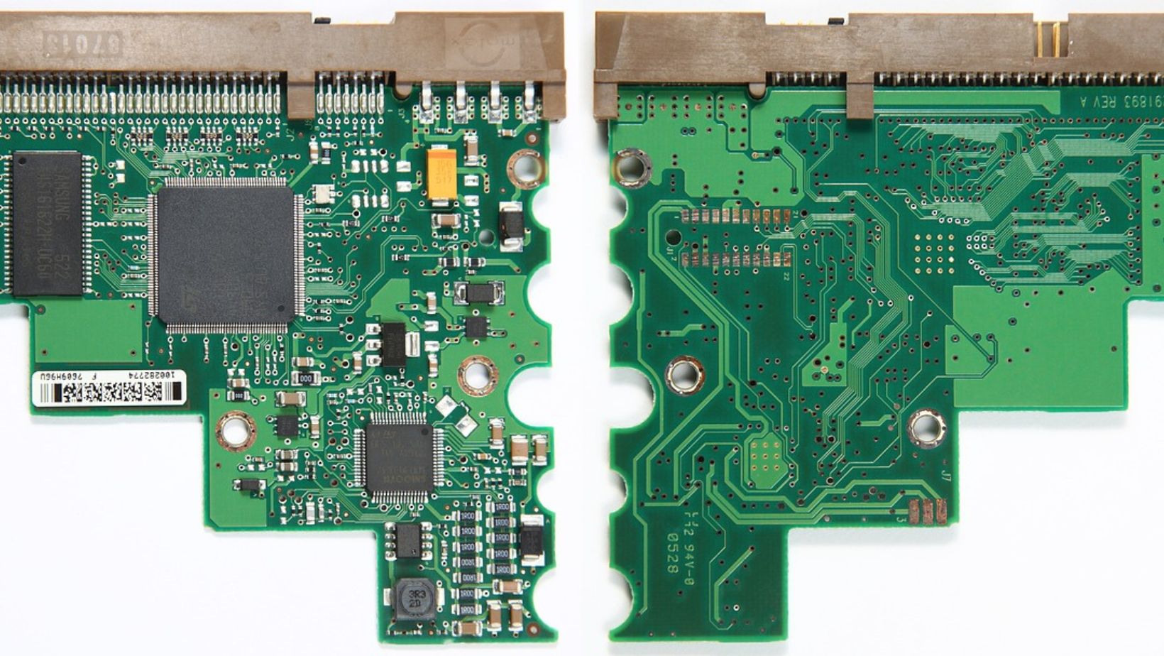
Printed circuit boards (PCBs) are prime suspects for every working technology around us. There you have your smartphone, your trusty laptop, or even smart fridge (but not yet smart enough to count your calories, but it’s getting there), and all the magic behind this amazing technology lies with the little fellows called PCBs.
Have you noticed how every new generation of laptops is lighter and faster to work with? How many smartphone models have larger memory and thinner lines? Those features are highly connected with creative solutions in PCB design.
The production is on the high rise too. For example, take Japan. Despite last years not being so valued in the market, the electronic products and components market is expected to have annual growth of -0.12% by the year 2029. At the same time, PCB manufacturing rate is predicted to grow by 2% through 2025. Basically, it seems that whatever happens to the market, PCB is going forward with a steady climb. And every step of the way is filled with new designs.
The Birth of a PCB
Let’s start with the basics a bit. You can imagine a PCB as a miniature city. The traces are like roads, the components are buildings, and the vias are underground tunnels. Our goal? To make this city as efficient, strong, and aesthetically pleasing as possible. Maybe one day this beauty goes to live in space. Who knows?
So, schematic design is the blueprint of your city. This is where all the magic starts. Engineers use CAD software to make a schematic diagram, which is essentially a roadmap of how all the components connect.
And components are like buildings. Building–placing components–isn’t just about cramming everything in. It’s about thoughtful urban planning, just like in the real city. For example, critical components like the CPU or memory modules often have prime real estate, while passive components like capacitors and resistors can fill in the gaps.
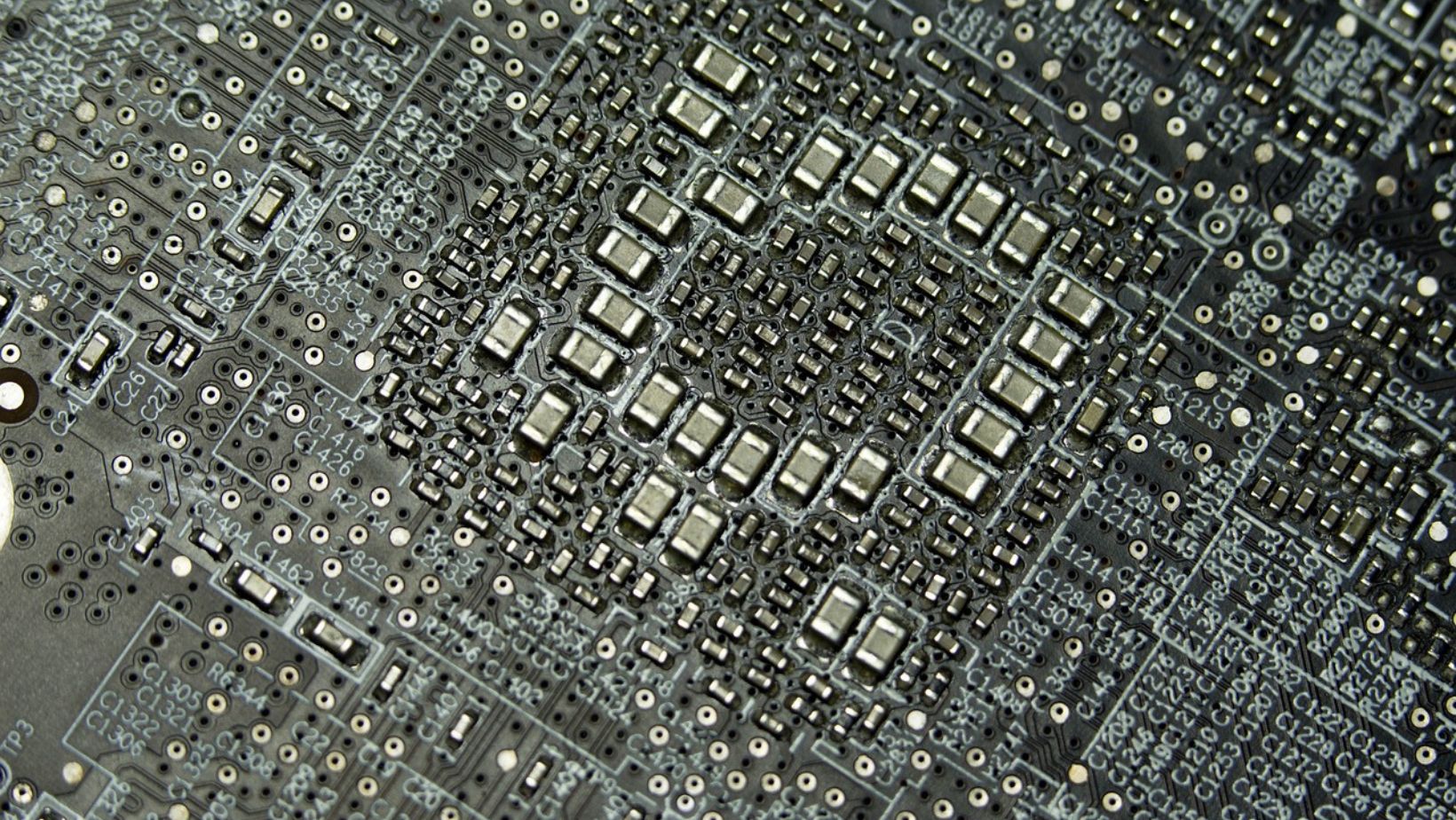
The most exciting part is routing. Here, we lay down the roads (traces) that connect everything. This is the part where engineers can be truly creative. They need to navigate the complex terrain of high-speed signals, electromagnetic interference, and power distribution. Sometimes, it feels like playing a 3D game of Tetris.
The Art of Miniaturization
Did you know that the very first PCB was made of copper coil? And now, some half-century later, there are various materials and designs. We all want our gadgets to be as thin and light as possible without sacrificing performance. Our wish for miniaturization has led engineers to be innovative when it comes to new PCB solutions.
The most popular nowadays are Rogers PCB materials and Fr-4. The common opinion is that Rogers PCBs are higher quality because of its specific layers, and the Fr-4 is the best when it comes to storing electrical energy or when you’re on budget.
High-density (HDI) PCBs pack more components into a smaller area by using finer lines and spaces, more layers, and smaller vias. It’s like a skyscraper in a PCB city, with more space to accommodate more inhabitants.
There are also blind and buried vias. Traditional vias go through the entire board, and it’s like drilling a hole from the roof of a building to the basement. Bud blind vias go only from one layer to an internal layer, and buried vias connect internal layers without reaching the surface. That way you have more space on the board.
Then, there are tiny tunnels that let signals pass between layers. They are smaller than traditional vias, like secret passages that let data zip around the PCB city.
Tackling Thermal Management
Electronics generate heat. It’s just the way it is. Managing this heat is important to make sure your devices have longer life and are more reliable. It’s like a summer city without air conditioning.
There are special thermal vias that act like ventilation shafts, which helps to dissipate heat from hotspots. They connect the heat-generating components to large copper areas on other layers that act like heat sinks.
Heat sinks and heat pipes are like air conditioning units for PBC City. They draw away heat from critical places and keep everything cool.
But sometimes it’s about material too. Engineers can use conductive adhesives or thermal pads to transfer heat away from components. It’s a more efficient way. It’s like upgrading from a hand fan to an industrial-strength cooler.
Signal Integrity and Electromagnetic Compatibility
PCB city is always busy with signaling data. These processes are fast and many. Making sure they don’t interfere with one another is a complex and fascinating challenge.
Think of impedance as the traffic rules for signal highways. Matching impedance makes sure that signals travel without distortion or reflection. This can happen because engineers use controlled impedance traces and adjust the width and spacing to keep things in line.
Some signals travel better in pairs. Differential pairs are two traces that carry the same signal but in opposite phases. With this technique, the noise is reduced and signal integrity is improved, which is important for high-speed data.
Then there is also shielding. Just like noise-canceling headphones, it helps block unwanted interference. Meanwhile, ground planes are big areas of copper connected to the ground, and they act as reference points for signals. They also reduce electromagnetic interference (EMI).
Flex and Rigid-flex PCBs
Flexibility might easily be the most important feature of PCBs new design. The flexible PCBs are, they can fit into unconventional shapes and sizes. This is something that most modern devices demand as a part of progress.
Flex PCBs are made from flexible materials like polyamide. They can bend and fold. It’s like Brus Lee came to tell them to be the river. They bend and fold through PCB city, just like a river, which allows for dynamic and space-saving design.
However, rigid PCBs have good features as well. Rigid-flex PCBs combine the best of both worlds. They have flexible sections to connect different parts, but rigid sections are for mounting components. In the PCB city, they look like strong buildings with adaptable bridges.
Advanced Manufacturing Techniques
With greater need for PCBs, there are better ways at manufacturing. Not to mention that complex designs demand complex processes to bring them to life.
Traditional mechanical drilling can’t handle the tiny visa needed for modern PCBs. But laser drilling is perfectly precise for microvials.
Before, engineers had to use traditional masks to create PCB traces, but now there is direct imaging. It uses UV light to transfer the design directly to the board.
3D printing is nother high manufacturing technique. Before it was used only for prototypes, but those days are long gone. Additive manufacturing can create complex PCB structures layer by layer. This method can open new possibilities for customization and design.
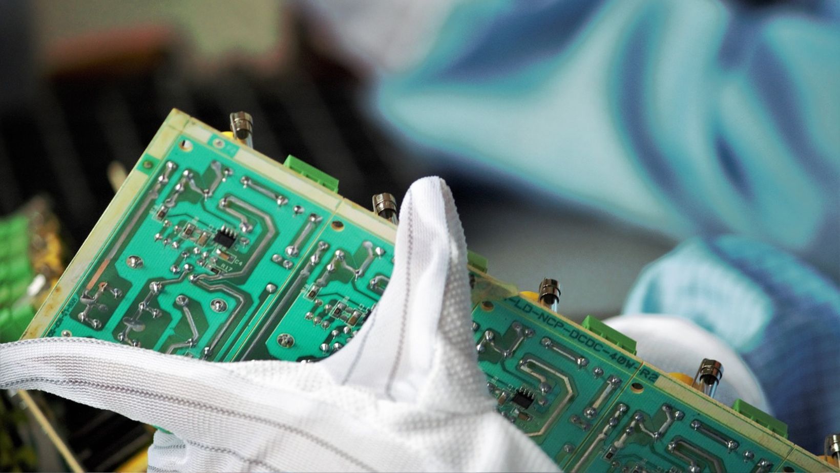
Testing and Reliability
Naturally, before PCB can be inhabited by electronic components, it needs to go through some serious testing.
Automated Optical Inspection (AOI) is a high-tech technique that uses pattern recognition and cameras to inspect PCBs for details.
In-circuit testing (ICT) checks the electrical performance of the PCB by probing different points.
So far it looks like your regular elderly person in pursuit for the perfect loaf of bread, inspecting it visually and by touching and squeezing it. But the next step is a bit tricky and is not recommended for trying at home.
Burn-in testing involves running the PCB at high temperatures and loads to weed out any early failures. It’s like sending your PCB to a boot camp where only the strongest survive. ANd strong PCBs are needed, considering for what purposes they’re used. They are not only part of your everyday gadgets but also instruments used in the automotive, marine, and aeronautic industry (including traveling to space). People’s lives depend on good technology that can withstand high and freezing temperatures both, pressures, and time.
What’s Next?
Have you seen the TV documentary where people said we need to catch up to alien technology? To be as modern as they are? Well, it seems we’re moving in the right direction.
Researchers are exploring biodegradable materials for PCBs which will reduce electronic waste. We also need wearable and implantable electronics, and sooner PCBs can cope with that, medicine for instance can go forward with prosthetics. Artificial Intelligence (AI) is also playing a part in PCBs designs. AI can optimize layouts and predict potential issues before they arise.
All in all, PCB design is a fascinating mix of art and science. Engineers never stop working on new designs, pulling one invention after another. They need to keep up with the high demands of the world (and aliens).
Imagine meeting outworlders with the same technology at hand, where you can transfer data and learn from each other at an equal level. Wouldn’t that be great?